What Is Deposition Science Definition Unlocking The Secrets Of Material Science At The Atomic Scale
What Is Deposition Science Definition Unlocking The Secrets Of Material Science At The Atomic Scale
Deposition science lies at the frontier of modern material engineering, representing the precise art and science of thin-film growth upon solid substrates. It is the foundational process behind technologies ranging from microelectronics and photovoltaics to advanced coatings and nanoscale sensors. Defined by the controlled deposition of atoms, molecules, or nanoparticles onto surfaces, this discipline unlocks the hidden mechanics of material behavior at the atomic scale—revealing how film structure, interface properties, and crystallinity dictate performance.
In a world driven by miniaturization and precision, understanding deposition science is no longer optional; it is essential for advancing cutting-edge applications.
At its core, deposition science involves the controlled delivery and adhesion of material layers onto a target substrate, typically in vacuum or low-pressure environments. The process transforms gaseous or vapor-phase precursors into solid films through phase transitions such as condensation, chemical reactions, or atomic rearrangement.
Whether initiating growth through physical vapor deposition (PVD), chemical vapor deposition (CVD), or atomic layer deposition (ALD), each method imposes unique atomic-scale constraints that influence film quality, uniformity, and functionality. As expert materials scientist Dr. Elena Torres notes, “Deposition science is not merely about coating a surface—it’s about orchestrating atomic-scale interactions to design materials with tailored properties.” This precise orchestration enables innovations like ultra-thin anti-reflective coatings on solar panels or high-purity coatings in semiconductor wafers.
The Foundation: Atomic-Scale Mechanisms
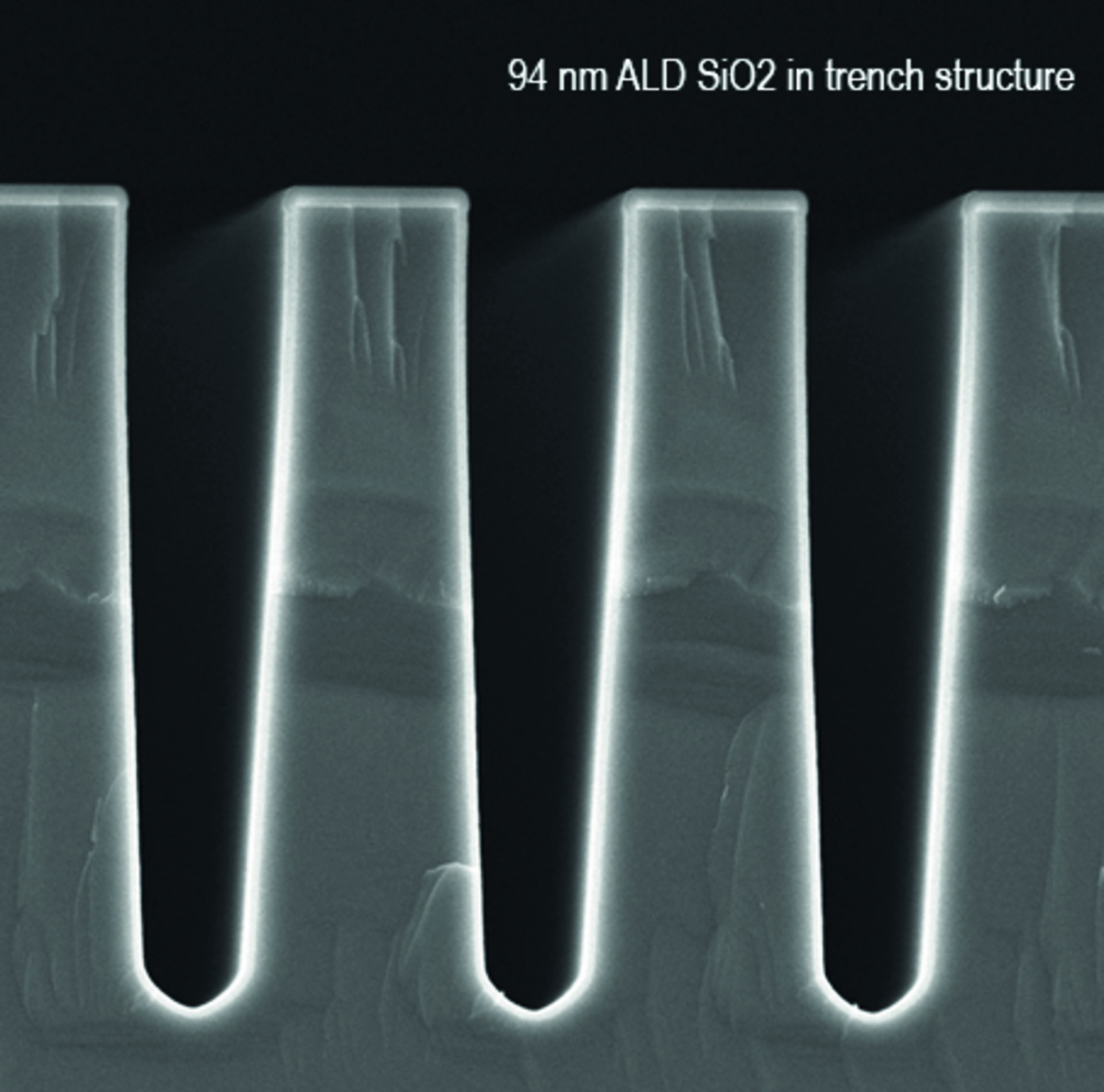
At the heart of deposition science is the behavior of atoms and molecules as they settle on a substrate. Growth dynamics are governed by factors such as surface diffusion, nucleation density, and adsorption energy, all of which determine whether a film forms with deterministic crystal orientation or chaotic amorphous structure. In chemical vapor deposition, for example, precursor molecules decompose on the surface, releasing reactive species that bond to form a continuous atomic lattice.In physical vapor deposition, lifted atoms from a target condense into thin films, with energy input carefully regulated to prevent defects. Atomic layer deposition stands out for its self-limiting reactions, enabling sub-nanometer control by alternating sequential gas pulses. “The atomic step-by-step assembly defines not only thickness but also electronic, optical, and mechanical attributes,” explains Dr.
Liam Chen, a leader in nanofilm research at the Advanced Materials Institute. This level of control allows scientists to engineer interfaces where charge transport or thermal stability matters most.
These atomic-level processes shape real-world performance in tangible ways.
Consider the case of gallium nitride (GaN) films deposited via plasma-assisted CVD for use in high-efficiency LEDs. The crystalline quality directly impacts light emission efficiency—disordered films scatter photons, reducing brightness and energy yield. Similarly, in protective coatings for aerospace components, deposition science ensures dense, pinhole-free layers that resist oxidation and extreme temperatures.
The ability to engineer grain boundaries, defect density, and strain at the atomic scale transforms passive surfaces into active functional interfaces, making materials smarter, stronger, and more durable.
Applications Driving Technological Progress
Deposition science fuels breakthroughs across industries, each application hinging on atomic-scale precision. In electronics, ALD-deposited high-k dielectrics overcome traditional scaling limits in semiconductor nm-scale transistors, enabling faster, more power-efficient processors.In renewable energy, thin-film CVD layers on perovskite solar cells enhance charge extraction and longevity. Meanwhile, biomedical devices leverage biocompatible thin films—deposited under ultra-clean conditions—to improve implant integration and drug delivery precision.
The versatility extends to emerging fields like flexible electronics and quantum computing.
Stretchable sensors rely on conformal, nanoscale coatings that maintain conductivity under mechanical strain. In quantum devices, deposition of epitaxial superconductor films at atomic precision preserves quantum coherence essential for qubit performance. These examples underscore deposition science’s role as a cornerstone of next-generation innovation.
Challenges and the Road Ahead
Despite its transformative potential, deposition science faces persistent challenges. Achieving uniformity across large substrates, minimizing defects, and reducing energy consumption remain critical hurdles. Real-time monitoring and feedback systems are advancing, enabling adaptive control during deposition to optimize film properties dynamically.Meanwhile, integration with machine learning promises predictive models that anticipate film behavior, accelerating development cycles. Sustainability is also gaining focus—researchers seek low-temperature, low-waste deposition methods using novel precursors. “We’re not just improving deposition; we’re redefining its environmental footprint,” notes Dr.
Aisha Patel, materials chemist at the National Institute of Applied Sciences.
Choosing deposition science as a lens reveals how the smallest atoms shape the largest technologies. It is a discipline where fundamental physics meets applied engineering, delivering solutions once deemed impossible.
From enabling invisible circuits in smartphones to paving the way for fusion energy infrastructure, deposition science continues to unlock hidden pathways in material innovation—one atomic layer at a time. The intricate dance of atoms in deposition processes is more than a technical process—it is the silent architect of the advanced materials defining modern life. As tools grow finer and understanding deeper, deposition science remains a key driver in crafting the future, layer by layer, one atomic bond at a time.


Related Post

Images of Nikki Catsouras: A Gripping Portrait of a Tragedy Captured in Time

From Sighed Silhouettes to Sleek Statement: The Rise of Jacob Elordi Beard

Pier 48 San Francisco: Where Drama Meets Modern Beauty at the Edge of the Bay

What Time Is It in Milwaukee? Precision in the Heart of Wisconsin Time Zone