The Gerber Revolution: Precision Engineering Meets Modern Manufacturing
The Gerber Revolution: Precision Engineering Meets Modern Manufacturing
At the heart of today’s advanced manufacturing lies a design standard so foundational yet rarely celebrated—the Gerber file. Originating from the pioneering work of Dr. Charles Gerber in the 1960s, this line specification format has become the invisible backbone of electronics, circuit design, and printed circuit board (PCB) fabrication.
Far more than a mere technical artifact, the Gerber file represents decades of innovation in precision, standardization, and digital workflows that power the global electronics industry.
The genesis of Gerber’s influence stems from his development of a simple yet revolutionary file format designed to encode the geometric layout of PCB traces and component placements. As Charles Gerber noted, “Accuracy in design is not a feature—it’s a necessity.” This philosophy embedded itself in the standard, enabling seamless communication between design software and manufacturing equipment.
Today, Gerber files serve as the universal language for PCB manufacturers, ensuring that every layer of a board—from copper pathways to solder mask outlines—is faithfully reproduced across continents and production scales.
From Lines to Layers: How Gerber Files Define Modern Electronics
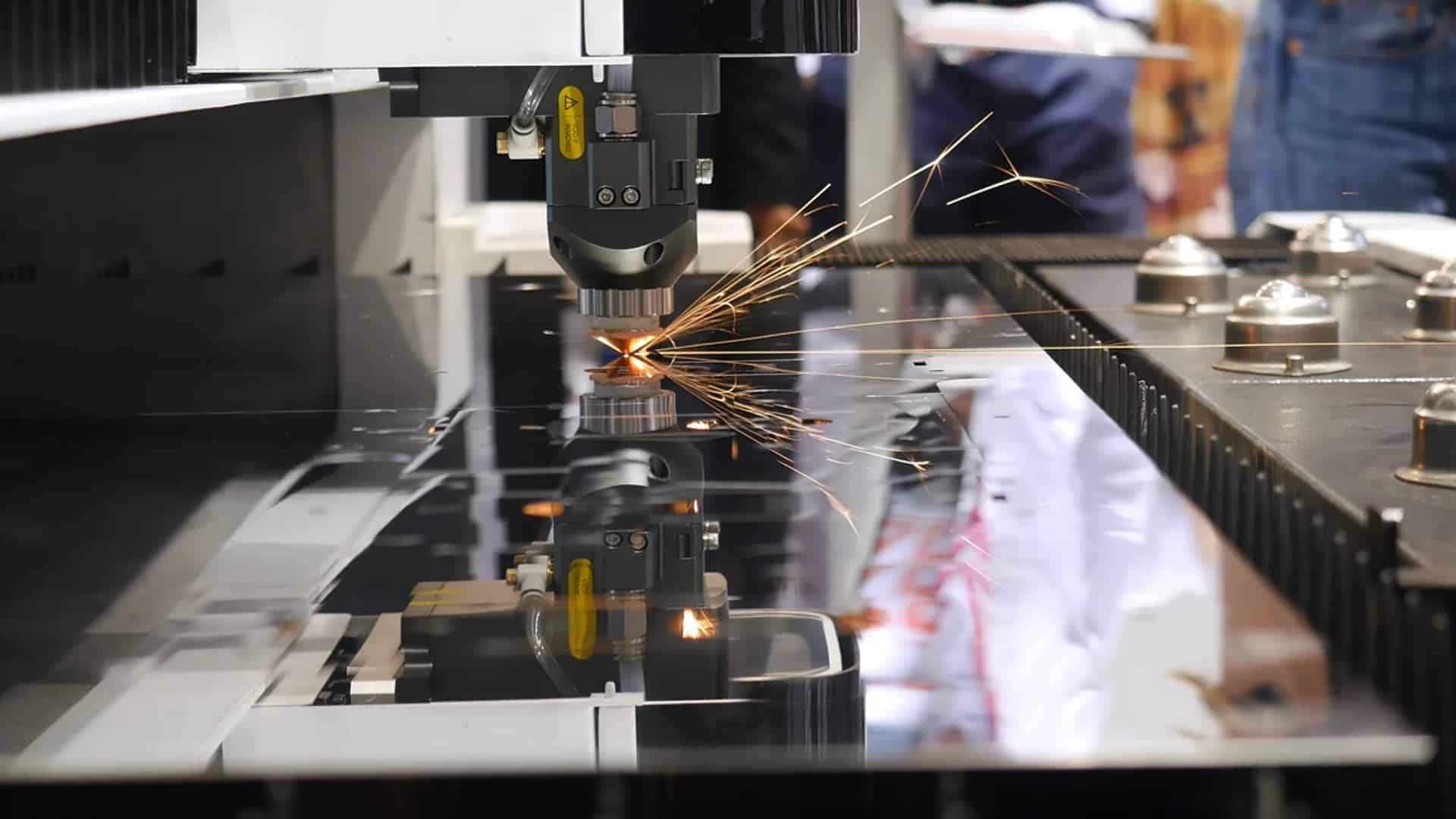
Gerber files are not just one-file-comes-a-round solutions; they encapsulate multi-layered complexity. A single PCB design comprises multiple layers—top conductive layer, internal signal layers, power and ground planes, and silkscreen annotations—all meticulously described in Gerber-compatible formats. These files specify exactly where copper should appear, where vias connect layers, and where resistor values are annotated.This level of detail ensures consistent quality across high-volume production runs, where even micron-level deviations could compromise functionality.
There are several core types of Gerber files, each serving a distinct purpose: - **PCB Source Files (.gb)**: Define the copper layout and track geometry, including polygon outlines and routing instructions. - **Silkscreen Files**: Specify text, logos, and component labels placed on the board surface. - **Solder Mask Files**: Outline protective layers that shield copper from short circuits while defining soldering zones.- **Bill of Materials (BOM) Integrations**: Increasingly linked with component databases to maintain traceability. “Gerber files bridge the gap between concept and capture,” explains Dr. Elena Torres, senior engineer at a leading electronics design firm.
“They ensure the transient idea in a CAD environment translates flawlessly into a manufacturable reality.” The format’s adaptability allows integration with advanced tools like 3D visualization software, PCB simulation suites, and automated fabrication machines—all operating under the same unified data structure.
Real-world implementation of Gerber workflows transforms manufacturing cycles. For example, in portable medical devices where miniaturization demands micron-level precision, Gerber-based design rules prevent trace misalignment that could cause signal delays or electrical faults.
Similarly, in automotive electronics, where reliability under thermal stress is critical, Gerber files support controlled impedance routing and thermal management through detailed layer stack descriptions.
Why Gerber Remains Indispensable in a Digital Age
Amid growing complexity in multi-layer PCBs and flexible electronics, the Gerber format retains dominance because of its stability and universal acceptance. While newer data standards like IPC-2581 and OASIS have emerged to support high-speed signals and 3D-printed components, Gerber continues to underpin over 90% of PCB production globally. This resilience stems from decades of industry investment, regulatory adherence, and an unshakable track record of compatibility.Yet, evolution is ongoing. Modern adaptations include enhanced metadata, encrypted security layers for IP protection, and tighter integration with artificial intelligence-driven design validation tools. As PCB designs grow denser—driven by 5G, AI, and IoT demands—Gerber’s role expands beyond layout encoding to active quality assurance, enabling real-time verification of design intent against manufacturing constraints.
The Future of Gerber: Precision Reimagined
Looking forward, the Gerber standard is not static; it is adapting to meet the demands of next-generation electronics. Innovations such as augmented reality (AR) integration with Gerber visualizations allow engineers to overlay design data directly onto physical boards during assembly, reducing human error. Moreover, cloud-based platforms are enabling collaborative workflows where multiple stakeholders access updated Gerber files in real time, accelerating time-to-market.“Gerber’s legacy is endurance through evolution,” notes Klaus Weber, product lead at a global PCB solutions provider. “It’s more than a file format—it’s a foundational infrastructure upon which entire industries build scalability, precision, and innovation.” As semiconductor miniaturization pushes geometric limits, the fidelity enabled by Gerber will only grow more critical, ensuring that the invisible lines defined by these files continue to shape the connected world. From humble beginnings in mid-20th century electronics, Gerber files have evolved into a global standard, underpinning the precision that pulses through every smartphone, automotive control unit, and medical implant.
Their story is not just one of technical utility but of consistent, unrelenting precision—where every line encoded in binary becomes a silent trust between design and manufacture. In an era of rapid technological change, Gerber endures not merely as a legacy format, but as a vital, adaptive force ensuring that complexity remains manageable and reliable—designed in detail, produced with accuracy.


Related Post

Gerber Meaning In Toronto: The Foundational Term Shaping Urban Design and Community Identity

Sabrina Carpenter's Iconic Headshot: The Face Behind the Rising Star

Iwan Rheon: The Dynamic Force Redefining Modern Acting in Global Theatre

49ers vs Lions: Decoding the Matchday Battle Through Player Stats That Defined a Giants-LIONS Clash


